In a furious competition to gain the first-mover advantage in 3-nanometer (nm) production for major customers like Apple and Nvidia, serving the high-performance computing (HPC) and smartphone sectors, TSMC is engaged with its closest foundry industry rival, Samsung.
From eastern Germany to southern Japan, construction of semiconductor production fabs, research and development centers, and processing units is in progress. Governments increased financing and subsidies for chip manufacturing all across the world as a result of the worldwide semiconductor shortage, which served as a reminder of how important semiconductor accessibility is in the modern economy.
In the industry of producing semiconductors, competition and advancement are constant, driving businesses to provide cutting-edge solutions. Leading company in the sector TSMC (Taiwan Semiconductor Manufacturing Company) has consistently led the way in technical development. The highly anticipated 3-nanometer (nm) chip technology has experienced substantial tool-related difficulties in recent TSMC efforts to develop and manufacture it. In this blog post, we go into TSMC's 3-nm push and examine the challenges they have encountered with tool development, as well as the solutions they have come up with.
In a furious competition to gain the first-mover advantage in 3-nanometer (nm) production for major customers like Apple and Nvidia, serving the high-performance computing (HPC) and smartphone sectors, TSMC is engaged with its closest foundry industry rival, Samsung. Recent claims of 3-nm leadership by TSMC in its quarterly results have heightened the already-intense rivalry between the two businesses.
To serve clients like Apple, Nvidia, and other businesses involved in designing data center CPUs, TSMC, Samsung, and Intel are all attempting to establish themselves as technological leaders. The extremely competitive foundry market, which has continuously outperformed the entire semiconductor industry in terms of growth for many years, will be dominated by the company that ultimately secures leadership status. Mehdi Hosseini, a senior equities research analyst at Susquehanna International Group, claims that TSMC continues to hold the top spot in this industry.
The process of developing tools to realize TSMC's 3-nm technology has run into a number of obstacles. The intricacy and accuracy needed to make instruments at such a small scale are a significant barrier. The tolerances for mistakes get exponentially tighter as chip size decreases, necessitating rigorous engineering and manufacturing methods.
The introduction of novel materials and procedures in TSMC's 3-nm technology has also made tool development more challenging. The engineering teams at TSMC have faced considerable obstacles in adapting current tools or creating new ones that can handle these developments.
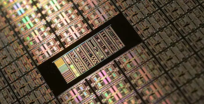
The iPhone A17 chip, which is anticipated to have a die size ranging from 100 to 110 mm square, will reportedly use 82 mask layers, according to a report by Arete Research. This predicts a yield of about 620 chips per wafer and a four-month wafer cycle. According to Arete, the M3 chip will have a die size of roughly 135 to 150 mm square, yielding 450 chips per wafer.
According to Simpson of Arete Research, TMSC’s main focus as it begins this early ramp-up is on optimizing yield and wafer cycle rates to boost operating efficiencies.
According to Hosseini, the adoption of multi-patterning using EUV (extreme ultraviolet) lithography from tool provider ASML has caused delays in the introduction and ramp-up of TSMC's 3-nm technology. Although efforts to lower the number of EUV multi-patterning layers by easing design restrictions have resulted in bigger die sizes, the cost-benefit analysis has been unfavorable due to the high cost of EUV multi-patterning. Hosseini further emphasizes that the availability of ASML's faster EUV system, the NXE:3800E, in the second half of 2023 will mark the actual scaling of the 3-nm node.
As per Hosseini's analysis, the introduction of the NXE:3800E is anticipated to increase wafer throughput by about 30% in comparison to the existing NXE:3600D, thereby lowering the overall cost of EUV multi-patterning.
As they scale their N3E and other versions of the 3-nm node to serve a wider range of customers, TSMC expects to expedite the deployment of the NXE:3800E in the first half of 2024, according to Hosseini.
The current industry chip inventory correction has, according to TSMC, surpassed their initial projections from three months ago and might continue into the third quarter of this year. As a result, TSMC now expects its revenue to shrink in 2023, which would be the first decline in almost ten years. According to TSMC, a leading indicator for the electronics sector, there could be a mid-single-digit percentage point decline in sales.